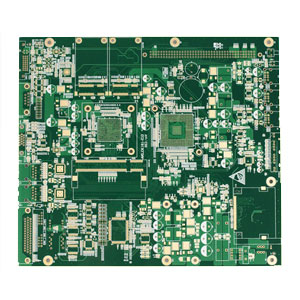
Product Detail:
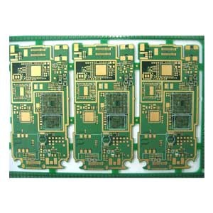
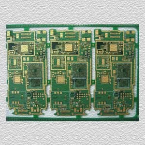
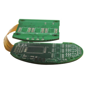
With our comprehensive strength in PCB manufacturing, Hecheng Fast Electronic Technology promptly provides low-cost, high-reliability high-level PCBs from our domestic and foreign production bases. By supporting fine pitches with high alignment accuracy technology and applying multi-layer stacked HDI technology using laser vias and filling plating, Hecheng Fast Electronic Technology has realized a multi-layer substrate structure with a high degree of wiring freedom. In addition, we have achieved a reduction in the number of layers and costs through tailor-made services from PCB design to implementation.

Benefits of high layers PCB
• High-density PCB with narrow pitch pattern and Vias with high-aspect ratio.
• Best design rule for customers’ low-loss transmission requirements.
• High Tg PCB for Pb free mounting, application requirements, etc.
Design Rule
High-speed transmission: Transmission-loss improvement
• Wide range of optimal low loss materials.
• Over 50Gbps signal transmission throughout the board.
• Chemical bonding technology to minimize the transmission loss
due to skin effect at high frequency.
High speed transmission: Reflection loss minimization
• Best structure to minimize reflection noise without open stub.
• Hybrid layer configuration composed of high density wiring layer and high speed low-loss transmission layer.
• Optimal design rules and layer structure at the early stage of PCB design.
 Hecheng Electronic Technology Group Limited

