Product Detail:
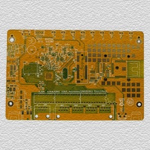
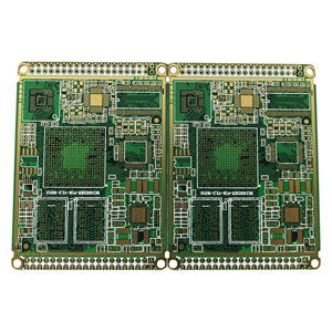
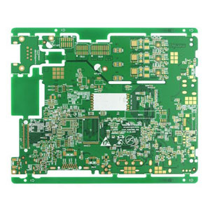
Holes for electronic components have to be plated through for conductivity on both the circuits. Conductive holes in the PCB allow circuits on one side to attach to circuits on the other side. Electronic components are soldered on both sides. Since, there are two or double conductive layer forming the circuit; it is called Double Sided PCB or Two Layer PCB.
Since 2012, we are growing from offering customers with single service of printed circuit boards to support comprehensive service with advanced circuits, mass PCB production, PCB assembly, parts purchasing in one stop PCB turnkey solutions. We also can produce quick turns to meet 24-hour delivery for high-quality double sided PCBs, 48-hour for 4 to 8 layers and 120-hour for 10 layer or higher PCBs. Our high quality PCBs come out from the raw material we choose, advanced equipment we use, process control we follow, qualified management abide by and all our professionals we have.

The difference between the double-sided PCB and single-sided PCB
Double sided printed circuit board is little complex than single sided printed circuit board. These types of PCB have one single layer of the base substrate but conductive layer on both sides of the substrate. Solder mask is applied on both sides of the board.
The production of double sided printed circuit board is different from that of single-sided printed circuit board. In addition to the manufacturing process, the double sided printed circuit board has an additional copper sinking process, that is, the process of conducting double sided printed circuit board.
 Hecheng Electronic Technology Group Limited


