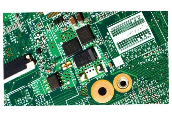
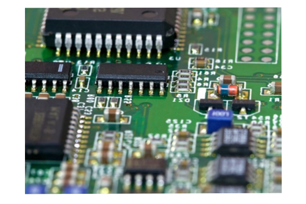
In the PCBA packaging process, solder mask is a very important coating material. Provides dielectric and mechanical shielding for PCBA boards during and after soldering and prevents solder deposits in this location. Generally, the two commonly used welding film materials in electronic processing plants are liquid film and dry film.

1. Pad through hole line. In principle, resistance soldering should be done on the wires between the vias that connect to the pads.
2. The resistance welding design between the pad, and the pattern specification of the resistance welding should conform to the design of the welding end distribution of the specific component. If windowed resistance welding is used between pads, the short circuit between pads will not occur.

4. There is no resistance welding film and no resistance welding hole under the module. After wave soldering, the solder on the hole may affect the reliability of IC soldering, and may also cause defects, such as short circuit of components.
The above are the factors that cause poor PCBA solder mask, I hope the above little knowledge can help you!
If you have any questions, please click PCBearth.com
 Hecheng Electronic Technology Group Limited
